
XT V Series – X-ray and CT Technology For Electronics Inspection
Price Available Upon Request
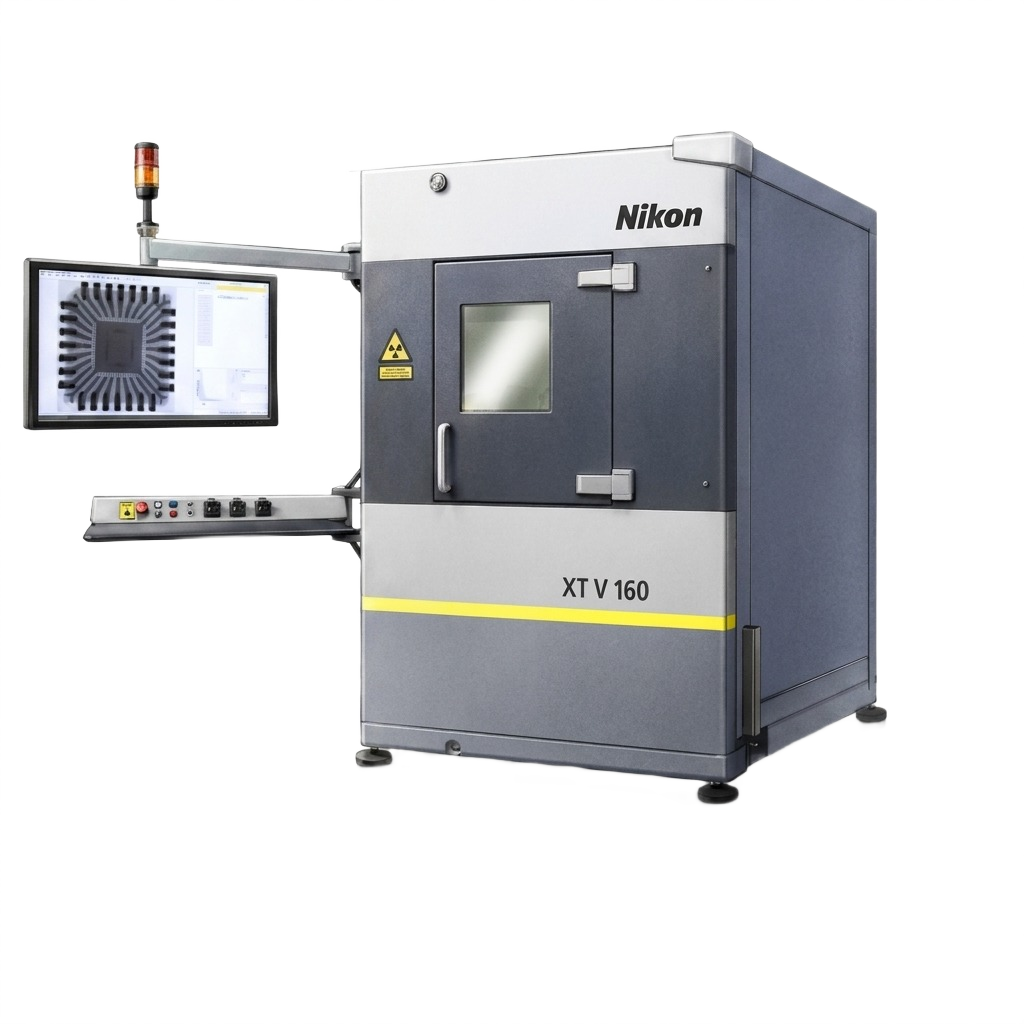
The Nikon XT V Series provides non-destructive X-ray and CT inspection for PCBs, BGAs, chips, and other electronic components, with configurations for electronics and semiconductor inspection. Available as XT V 160 and XT V 130C, the range combines high-resolution imaging, automated inspection through Inspect-X, PCB analysis, flexible viewing angles, and protective features including collision avoidance, Low Dose Collimator, and ESD Safety Upgrade.
Nikon XT V Series – X-ray and CT Technology for Electronics Inspection
The Nikon XT V Series comprises X-ray and CT systems for non-destructive inspection of electronic components and assemblies, including PCBs, BGAs, and chips. Designed for electronics and semiconductor inspection, the range supports applications across R&D, QA, QC, and failure analysis, depending on configuration.
Available as XT V 160 and XT V 130C, the series combines high-resolution X-ray imaging, intuitive inspection workflows, automated analysis capabilities, and flexible sample positioning for detailed internal inspection without damaging the component.
Automated Electronics Inspection
The XT V Series works with the Inspect-X interface to simplify inspection setup and operation. Automated inspection programs can be configured without programming, while the PCB Analysis Suite supports advanced measurement and analysis of:
- BGA
- Bond wires
- PTH
- Complex packages such as PoP on multi-layered boards
- Automated pass/fail inspection
- Automated reporting
These capabilities support both routine inspection and detailed electronics analysis.
High-Resolution X-ray Imaging
Nikon’s Xi microfocus X-ray sources are designed to provide sharp, stable, and bright X-ray images.
The supplied imaging features include:
- Diamond Window for improved contrast across the operating range
- In-house open tube design with integral generator
- High Contrast Filter 2.0 for simultaneous visibility of high- and low-contrast areas
- Detailed inspection of internal electronic structures and defects
The XT V 160 provides submicron feature recognition, while the XT V 130C provides micron-level feature recognition.
Flexible Sample Manipulation
The XT V Series uses a vertical system configuration with the X-ray source below the sample tray and a tilting imager above.
Inspection can be controlled through Inspect-X software or precise joystick manipulation. Intelligent motion control maintains the region of interest in view during 360° sample rotation, including at oblique viewing angles.
Model-specific viewing capability includes:
- XT V 160: Up to 82° in any direction
- XT V 130C: Up to 79° in any direction
Sample & System Protection
The XT V Series incorporates functionality intended to protect both the inspection system and sensitive electronic samples.
Features include:
- Automatic collision avoidance to help prevent physical damage to the system and sample
- Low Dose Collimator to minimise X-ray exposure during inspection of semiconductor devices
- ESD Safety Upgrade for protection of sensitive components and compliance with global standards
XT V 160 vs XT V 130C
| Specification | XT V 160 | XT V 130C |
|---|---|---|
| Maximum kV | 160 kV | 130 kV |
| Feature recognition | Submicron | Micron-level |
| Viewing angle range | Up to 82° in any direction | Up to 79° in any direction |
| Primary applications | Automated and real-time electronics and semiconductor inspection for R&D, QA, QC and failure analysis | Real-time electronics inspection |
Additional XT V 160 Specifications
The following technical information is explicitly supplied for the XT V 160:
| Specification | XT V 160 |
|---|---|
| X-ray source | Open tube with replaceable filaments for unlimited lifetime |
| High voltage generator | Integrated generator – no HV cable maintenance required |
| Sample tray | Carbon fibre tray, 580 mm (22.8 “) diameter |
| Cabinet dimensions (W x D x H) | 1,260 x 1,789 x 1,904 mm (50 x 70 x 75 “) |
| System weight | 2,100 kg (4,630 lbs) |
| ESD safety | ESD-safe to industry standards with optional ESD Safety Upgrade |
Electronics & Semiconductor Applications
The supplied applications identify the XT V Series for use in:
- Electronics
- Semiconductor
- Quality Laboratories
- Research and Development
The systems support inspection of complex electronic assemblies, including defect detection in BGAs and analysis of bond wire integrity. The PCB Analysis Suite also supports analysis of PTH and PoP packages on multi-layered boards.
| Weight | 2100 kg |
|---|---|
| Dimensions | 126 × 178.9 × 190.4 cm |
| Choose Variant | XT V 130C, XT V 160 |
Related products


Reviews
There are no reviews yet.